- 您现在的位置:买卖IC网 > Sheet目录495 > OP525DA (TT Electronics/Optek Technology)PHOTODARLINGTON NPN CLR 1210 SMD
�� �
�
�Silicon� Phototransistor� and� Photo� Darlington�
�in� 1210� SMD� Package�
�OP525,� OP525DA,� OP525F�
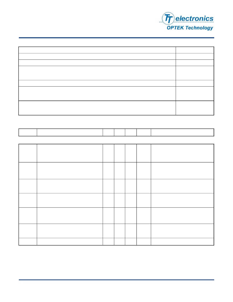
�Absolute� Maximum� Ratings� (T� A� =25°C� unless� otherwise� noted)�
�Storage� Temperature� Range�
�Operating� Temperature� Range�
�Lead� Soldering� Temperature� (1)�
�Collector-Emitter� Voltage�
�OP525,� OP525F�
�OP525DA�
�Emitter-Collector� Voltage�
�Collector� Current�
�OP525,� OP525F�
�OP525DA�
�Power� Dissipation� (2)�
�OP525,� OP525F�
�OP525DA�
�Electrical� Characteristics� (T� A� =� 25� °� C� unless� otherwise� noted)�
�-40� o� C� to� +100� o� C�
�-40� o� C� to� +80� o� C�
�260°� C�
�30� V�
�35� V�
�5V�
�20� mA�
�30� mA�
�75� mW�
�100� mW�
�SYMBOL�
�PARAMETER�
�MIN�
�TYP�
�MAX�
�UNITS�
�TEST� CONDITIONS�
�Input� Diode�
�I� C(ON)�
�V� CE(SAT)�
�On-State� Collector� Current�
�OP525F�
�OP525�
�OP525DA�
�Collector-Emitter� Saturation� Voltage�
�OP525,� OP525F�
�OP525DA�
�2.0�
�1.0�
�10.0�
�-�
�-�
�-�
�-�
�-�
�-�
�-�
�-�
�-�
�-�
�0.4�
�1.7�
�mA�
�V�
�V� CE� =� 5.0� V,� E� E� =� 0.5� mW/cm� 2�
�V� CE� =� 5.0� V,� E� E� =� 1.5� mW/cm� 2� (3)�
�V� CE� =� 5.0� V,� E� E� =� 0.15� mW/cm� 2� (3)�
�I� C� =� 100� μA,� E� E� =� 1.0� mW/cm� 2� (3)�
�I� C� =� 1� mA,� E� E� =� 0.5� mW/cm� 2� (3)�
�Collector-Emitter� Dark� Current�
�I� CEO�
�OP525,� OP525F�
�OP525DA�
�-�
�-�
�100�
�200�
�nA�
�V� CC� =� 10.0� V� (4)�
�Collector-Emitter� Breakdown� Voltage�
�V� BR(CEO)�
�OP525,� OP525F�
�OP525DA�
�30�
�35�
�-�
�-�
�V�
�I� C� =� 100� μA,� E� E� =� 0�
�I� C� =� 1� mA,� E� E� =� 0�
�Emitter-Collector� Breakdown� Voltage�
�V� BR(ECO)�
�OP525,� OP525F�
�OP525DA�
�5�
�5�
�-�
�-�
�-�
�-�
�V�
�I� E� =� 100� μA,� E� E� =� 0�
�I� E� =� 100� μA,� E� E� =� 0�
�Rise� and� Fall� Times�
�t� r,� t� f�
�λ� 0.5�
�OP525,� OP525F�
�OP525DA�
�Spectral� Bandwidth� OP525F�
�-�
�750�
�15�
�50�
�-�
�-�
�-�
�1100�
�μs�
�nm�
�I� C� =� 1� mA,� R� L� =� 1K� ?�
�I� C� =� 1� mA,� R� L� =� 1K� ?�
�-�
�Notes:�
�1.� Solder� time� less� than� 5� seconds� at� temperature� extreme.�
�2.� Derate� linearly� at� 1.33� mW/°� C� above� 25°� C.�
�3.� Light� source� is� an� unfiltered� GaAs� LED� with� a� peak� emission� wavelength� of� 935� nm� and� a� radiometric� intensity� level� which� varies� less�
�than� 10%� over� the� entire� lens� surface� of� the� phototransistor� being� tested.�
�4.� To� calculate� typical� collector� dark� current� in� μA,� use� the� formulate� I� CEO� =� 10� (0.04� t� -� ?)� ,� where� T� A� is� the� ambient� temperature� in� °� C.�
�OPTEK� reserves� the� right� to� make� changes� at� any� time� in� order� to� improve� design� and� to� supply� the� best� product� possible.�
�OPTEK� Technology� Inc.� —� 1645� Wallace� Drive,� Carrollton,� Texas� 75006�
�Phone:� (972)� 323-2200� or� (800)� 341-4747� FAX:� (972)� 323-2396� sensors@optekinc.com� www.optekinc.com�
�Issue� F�
�05/2012�
�Page� 3� of� 5�
�发布紧急采购,3分钟左右您将得到回复。
相关PDF资料
OP535C
PHOTODARLINGTON SILICON NPN T-1
OP538FC
PHOTODARL SILCN NPN FLAT SD LOOK
OP550D
PHOTOTRANS SILICON NPN SIDE LOOK
OP555D
PHOTOTRNS NPN PLASTIC SIDE LOOK
OP560C
PHOTODARLINGTON NPN 935NM SIDELK
OP565B
PHOTODARL SILICON NPN SIDE LOOK
OP573
PHOTOTRANSISTOR NPN SND REV GULL
OP580DA
PHOTODARLINGTON NPN CLR PLCC-2
相关代理商/技术参数
OP525F
功能描述:光电晶体管 Phototransistor RoHS:否 制造商:OSRAM Opto Semiconductors 最大功率耗散:165 mW 最大暗电流:200 nA 封装 / 箱体:T-1
OP526,005
功能描述:MOSFET OP526/UNCASED/FOIL// RoHS:否 制造商:STMicroelectronics 晶体管极性:N-Channel 汲极/源极击穿电压:650 V 闸/源击穿电压:25 V 漏极连续电流:130 A 电阻汲极/源极 RDS(导通):0.014 Ohms 配置:Single 最大工作温度: 安装风格:Through Hole 封装 / 箱体:Max247 封装:Tube
OP528,005
功能描述:MOSFET OP528/UNCASED/FOIL// RoHS:否 制造商:STMicroelectronics 晶体管极性:N-Channel 汲极/源极击穿电压:650 V 闸/源击穿电压:25 V 漏极连续电流:130 A 电阻汲极/源极 RDS(导通):0.014 Ohms 配置:Single 最大工作温度: 安装风格:Through Hole 封装 / 箱体:Max247 封装:Tube
OP529,005
功能描述:MOSFET OP529/UNCASED/FOIL// RoHS:否 制造商:STMicroelectronics 晶体管极性:N-Channel 汲极/源极击穿电压:650 V 闸/源击穿电压:25 V 漏极连续电流:130 A 电阻汲极/源极 RDS(导通):0.014 Ohms 配置:Single 最大工作温度: 安装风格:Through Hole 封装 / 箱体:Max247 封装:Tube
OP530
制造商:OPTEK 制造商全称:OPTEK 功能描述:NPN SILICON PHOTODARLINGTON
OP530FC
制造商:未知厂家 制造商全称:未知厂家 功能描述:Optoelectronic
OP530T,005
功能描述:MOSFET OP530T/UNCASED/FOIL/ RoHS:否 制造商:STMicroelectronics 晶体管极性:N-Channel 汲极/源极击穿电压:650 V 闸/源击穿电压:25 V 漏极连续电流:130 A 电阻汲极/源极 RDS(导通):0.014 Ohms 配置:Single 最大工作温度: 安装风格:Through Hole 封装 / 箱体:Max247 封装:Tube
OP531/A,005
功能描述:MOSFET OP531/UNCASED/FOIL//A RoHS:否 制造商:STMicroelectronics 晶体管极性:N-Channel 汲极/源极击穿电压:650 V 闸/源击穿电压:25 V 漏极连续电流:130 A 电阻汲极/源极 RDS(导通):0.014 Ohms 配置:Single 最大工作温度: 安装风格:Through Hole 封装 / 箱体:Max247 封装:Tube